Joystick Breakout PCB Rev 2.0 — Real Footprint, Real Pinout, Real Autoroute
Yesterday's joystick breakout PCB shipped with three quietly serious bugs: a hand-drawn switch footprint with the wrong pad geometry, a wire pad that physically overlapped a mounting hole, and a pinout I'd half-invented because I hadn't read the Alps datasheet diagram. Rev 2.0 fixes all three by stealing real reference designs and runs the full autorouter pipeline headless from the CLI.
What was wrong with Rev 1.0
The original board parsed-but-broken in three ways:
- Made-up footprint geometry. The SKRHABE010 has six SMD pads on diagonals (the body is a chamfered octagon). My Rev 1 footprint had axis-aligned pads on the wrong faces of the body. A real chip soldered to that footprint would have hit zero of its pads.
- Drilled-through-the-mounting-hole. Wire pad J1.6 (GND) was at (102, 116) and one of the M3 mounting holes was at (102.5, 117.5). The edges overlapped by ~0.9 mm. Either the JLCPCB drill operator catches it and rejects the board, or it doesn't and the GND pad has a hole through it.
- Hallucinated pinout. I had labelled SW1.2 as
DOWN, SW1.5 asCENTER, and SW1.6 asCOM/GND. The Alps datasheet circuit diagram says SW1.2 is Center (the press-down contact), SW1.5 is Common (the GND return), and SW1.6 is D (a directional). Three of six pin assignments were wrong.
The fix: stop guessing, start cloning
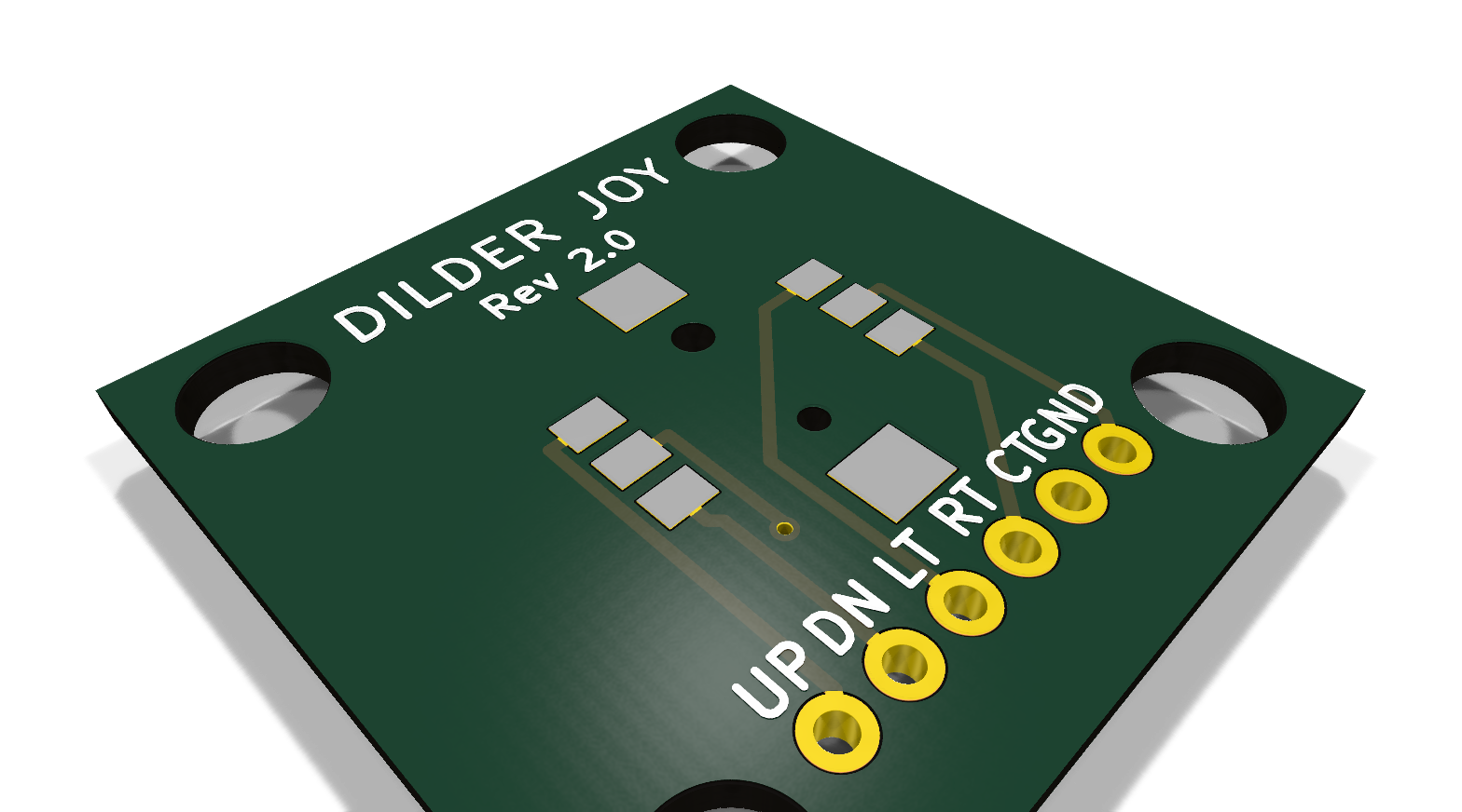
Footprint — cloned from crides/kleeb
The crides/kleeb keyboard library has a production-tested SKRHA-boss footprint used in real shipping keyboards. I copied its pad coordinates verbatim, then mathematically rotated everything -45° so the pads land on left/right faces of the body (instead of kleeb's diagonal arrangement which suits keyboard layouts but not breakouts). The two NPTH alignment-post holes (1.05 mm and 0.75 mm — the bumps on the bottom of the SKRHABE010 that locate it on the PCB) and the two SMD anchor pads carried over unchanged.
The clearances were verified before any pads went on the board:
Wire pad ↔ M3 mounting hole (drill-to-drill):  0.74 mm
Wire pad ↔ adjacent wire pad pitch:            1.00 mm
Switch courtyard ↔ M3 hole (edge-to-edge):     2.07 mm minimum
NPTH alignment hole ↔ nearest signal pad:      3.61 mm
Pad ↔ board edge:                              2.30 mm
All comfortably above JLCPCB's 0.2 mm minimums. No drills overlap.
Pinout — confirmed against the Alps datasheet circuit diagram

The pin function table, copied straight off the datasheet:
| SW1 Pin | Datasheet | Function | Net |
|---|---|---|---|
| 1 | A | direction (paired with C) | JOY_UP |
| 2 | Center | press-down contact | JOY_CENTER |
| 3 | C | direction (paired with A) | JOY_DOWN |
| 4 | B | direction (paired with D) | JOY_LEFT |
| 5 | Common | shared return for all 5 | GND |
| 6 | D | direction (paired with B) | JOY_RIGHT |
The schematic library symbol is now a copy of kleeb's switch:SKRHA symbol with the names matched to the datasheet (A/Center/C/B/Common/D). Cardinal — a shipping split keyboard at Painterman/Cardinal — uses the same symbol with the same pin numbering, which is the cross-reference that confirms it.
Headless autoroute — KiCad to Freerouting to KiCad, all from the CLI
The other big change: Rev 2.0 was routed entirely from a shell script. KiCad's built-in autorouter has been gone since v6, and the standard advice is to use Freerouting from inside the KiCad GUI. But Freerouting also has an undocumented-but-supported headless CLI, and the project ships an official Docker image that bundles a JRE — so the whole loop runs without installing Java locally.
# 1. Export Specctra DSN from the KiCad PCB (uses the pcbnew Python module)
python3 -c "
import pcbnew
b = pcbnew.LoadBoard('joystick-pcb.kicad_pcb')
pcbnew.ExportSpecctraDSN(b, '/tmp/joystick.dsn')
"

# 2. Run Freerouting headless
docker run --rm -v /tmp:/work \
  --entrypoint java ghcr.io/freerouting/freerouting:latest \
  -jar /app/freerouting-executable.jar \
  -de /work/joystick.dsn -do /work/joystick.ses -mp 100

# 3. Import the .ses session back into the board
python3 -c "
import pcbnew
b = pcbnew.LoadBoard('joystick-pcb.kicad_pcb')
pcbnew.ImportSpecctraSES(b, '/tmp/joystick.ses')
b.Save('joystick-pcb.kicad_pcb')
"

# 4. Verify with the KiCad CLI DRC
kicad-cli pcb drc --output drc.json --format json joystick-pcb.kicad_pcb
The Docker image's normal entrypoint is for API-server mode, hence the --entrypoint java override to drop into CLI mode.
The result
Freerouting reports:
- 23 trace segments + 1 through-hole via, total length 534 mm
- 8 bends, all 45° — zero 90° corners
- 0 clearance violations
- All 6 nets fully connected
KiCad's CLI DRC reports:
- 0 copper-clearance violations
- 0 unconnected ratlines
- 0 schematic-parity issues
The only DRC items remaining are 6 informational warnings about a missing joystick-pcb footprint library declaration (we use inline footprints with that namespace prefix) and KiCad 10's stock MountingHole differing from the embedded copy. Neither blocks fabrication.
Top + bottom
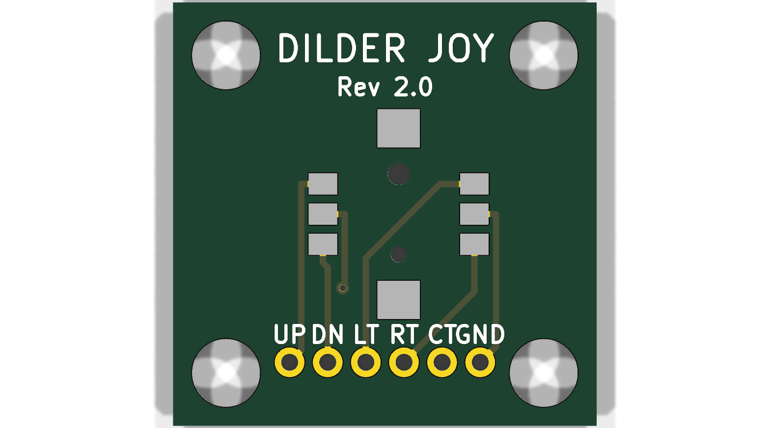
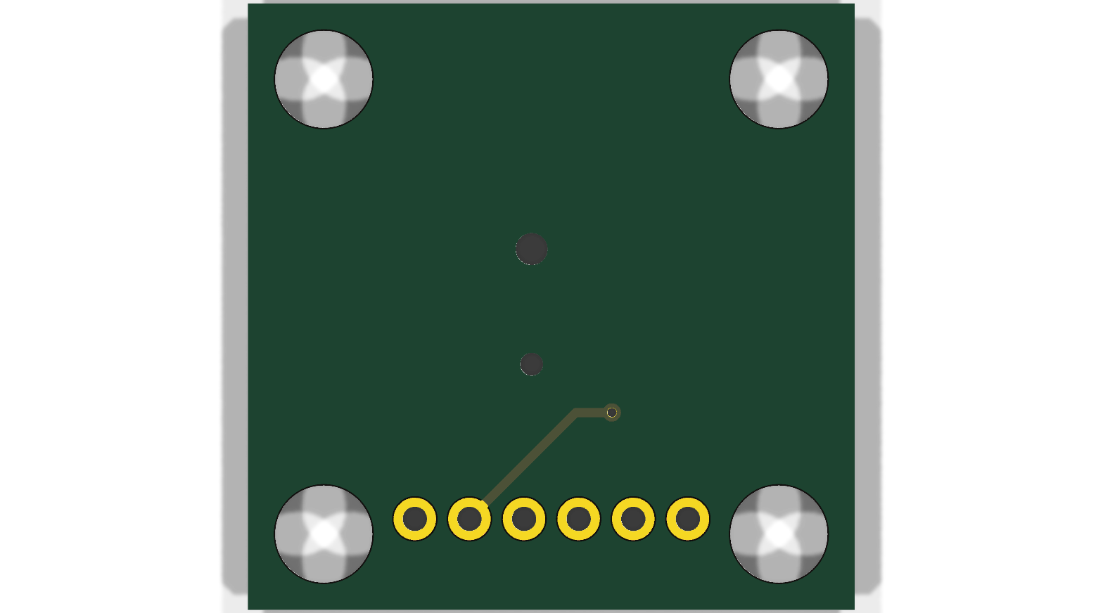
The top side carries most of the routing and the SKRHABE010 footprint with its two anchor pads (top/bottom of the diamond body). The bottom side has the via and the second routing layer Freerouting used to clear the body courtyard.
What I learned (and wrote down)
The pattern across all three Rev 1 bugs was the same: I'd guessed at a real-world dimension or pin assignment instead of pulling it from a datasheet or a known-good reference design. Once I started literally cloning kleeb's symbol and reading the Alps circuit diagram, the bugs evaporated.
To make this less of an ad-hoc lesson, I wrote up the broader prototyping discipline as hardware-design/HARDWARE-DESIGN-PROCESS.md — it covers both the SCAD-print loop (where the print-waste tax has been real) and the PCB loop (where machine-checkable gates kept this redesign clean), with a list of concrete process improvements pulled from this session's failures.
Files
hardware-design/joystick-pcb/joystick-pcb.kicad_sch— schematic with the cloned kleeb symbol, datasheet-confirmed pin names, six wire-stub labels per sidehardware-design/joystick-pcb/joystick-pcb.kicad_pcb— fully-routed Rev 2 PCB (23 segments, 1 via, all 45°)hardware-design/joystick-pcb/design-notes.md— pinout table, clearance table, headless Freerouting workflow, footprint provenancehardware-design/scad Parts/README.md— new — documents the three SCAD helper scripts (scad-export.py,bake-preset.py,export-preset.py)hardware-design/HARDWARE-DESIGN-PROCESS.md— new — prototyping discipline doc