Dilder Full Board Rev 1 — One Green Rectangle to Rule Them All
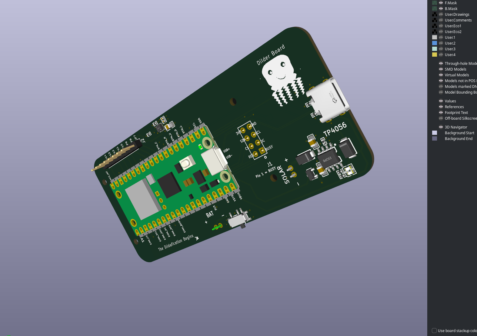
After two months of breadboards, flying wires, hot-glued battery clips, and a stack of off-the-shelf modules taped to the inside of a 3D-printed case, the Dilder is finally a single board. One PCB. One green rectangle the size of a chocolate bar. Everything the octopus needs to live, lives on it.
This is a huge milestone, so this post is the friendly tour — what got built, what got learned, and why the silkscreen says "The Dildafication Begins" on the front.
What's actually on the board
Imagine the Dilder up to this point as a clattering bag of parts: a tiny Pico computer, a charger module, a battery, a little gyro sensor, a 5-way joystick switch, a piezo speaker, a slide switch, a USB-C port, an e-paper screen — all wired together with rainbow jumpers. Rev 1 of the Dilder Full Board is the moment all of those parts get a permanent home next to each other, with the wires baked into the copper of the board itself.
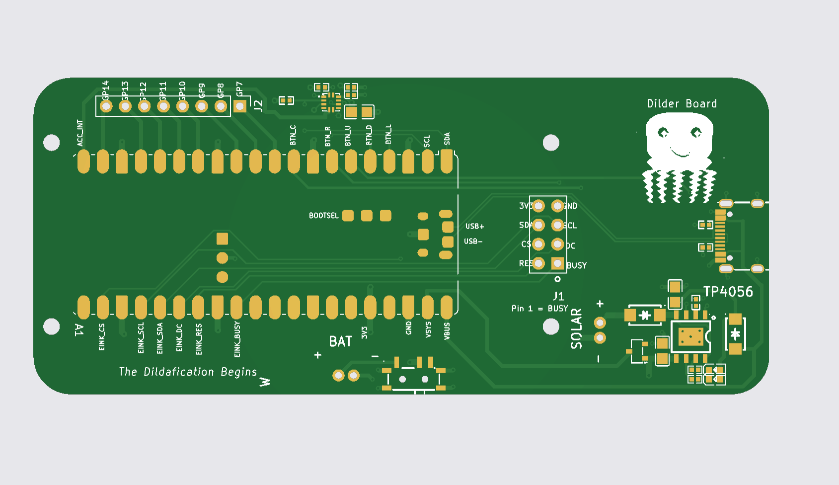
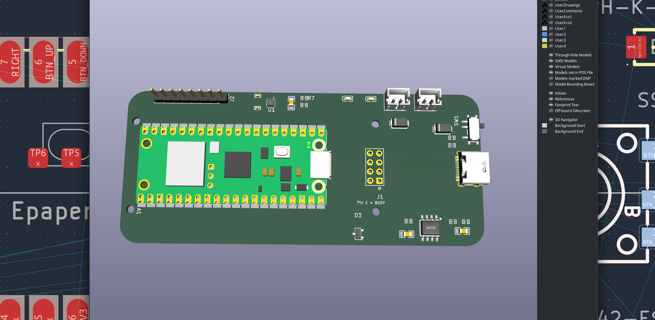
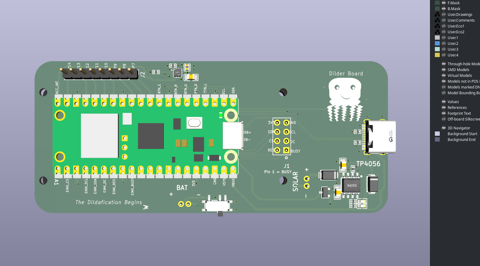
The front of the board carries the brain (a Raspberry Pi Pico 2 W), the charger circuit (TP4056), the USB-C port, the e-paper screen connector, a row of test pads for the buttons, the gyro, and a small mascot drawing of the octopus winking at the user.
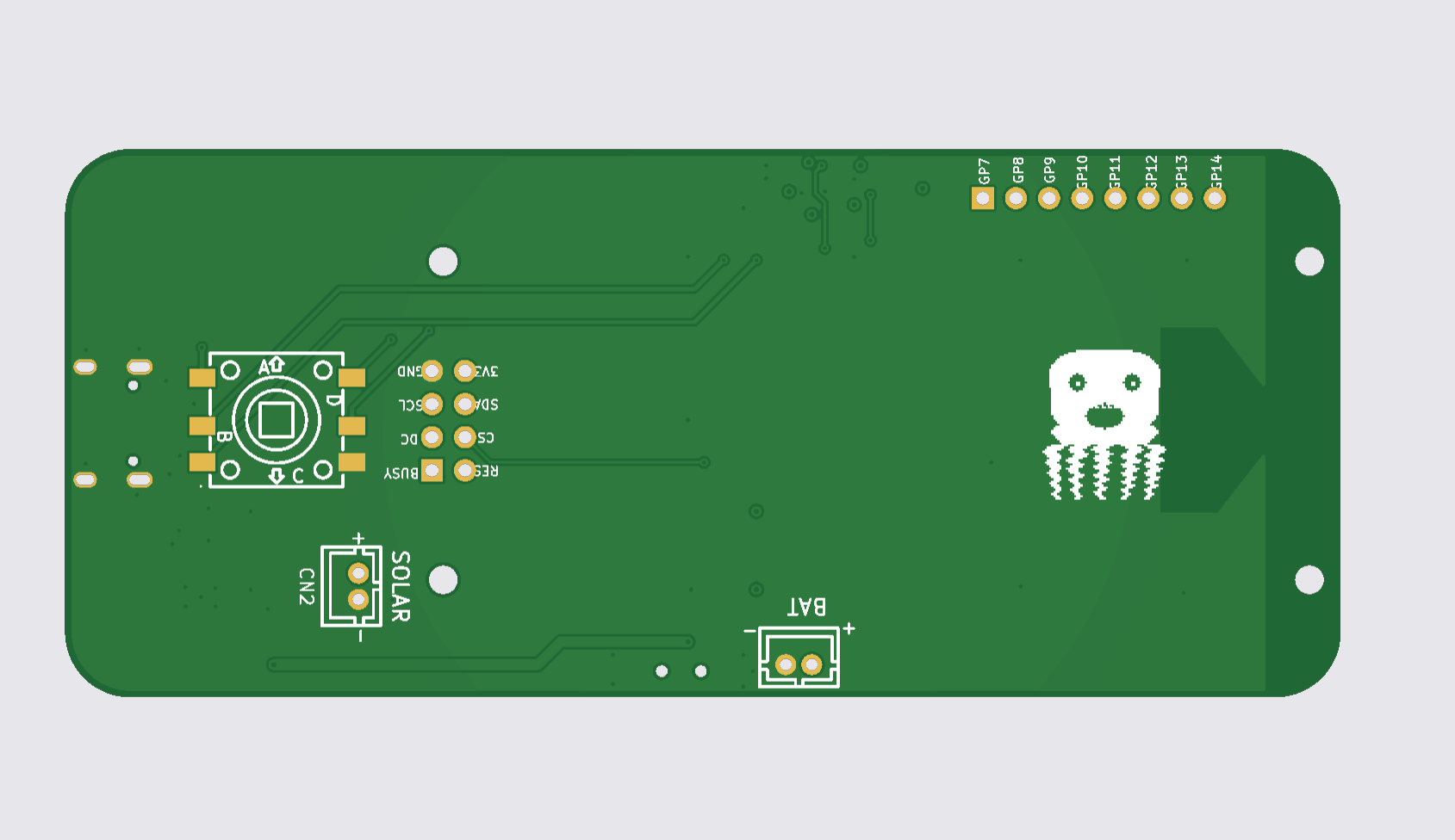
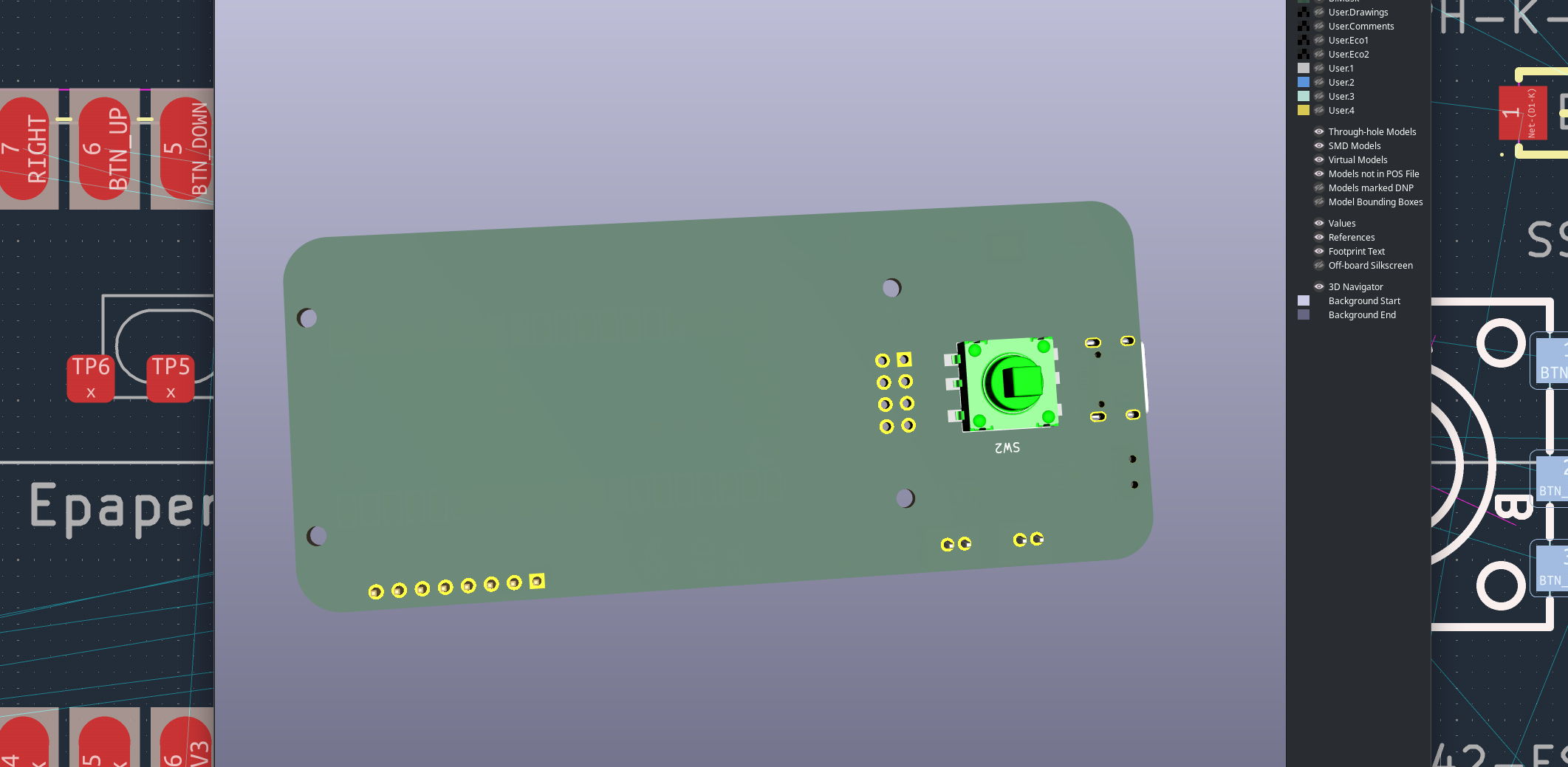
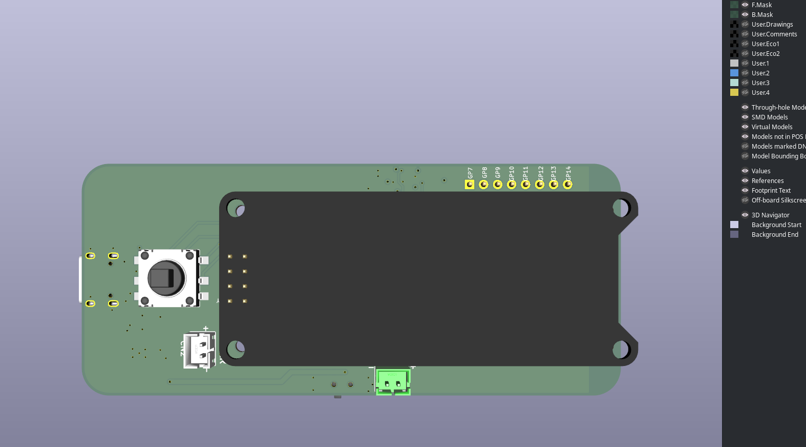
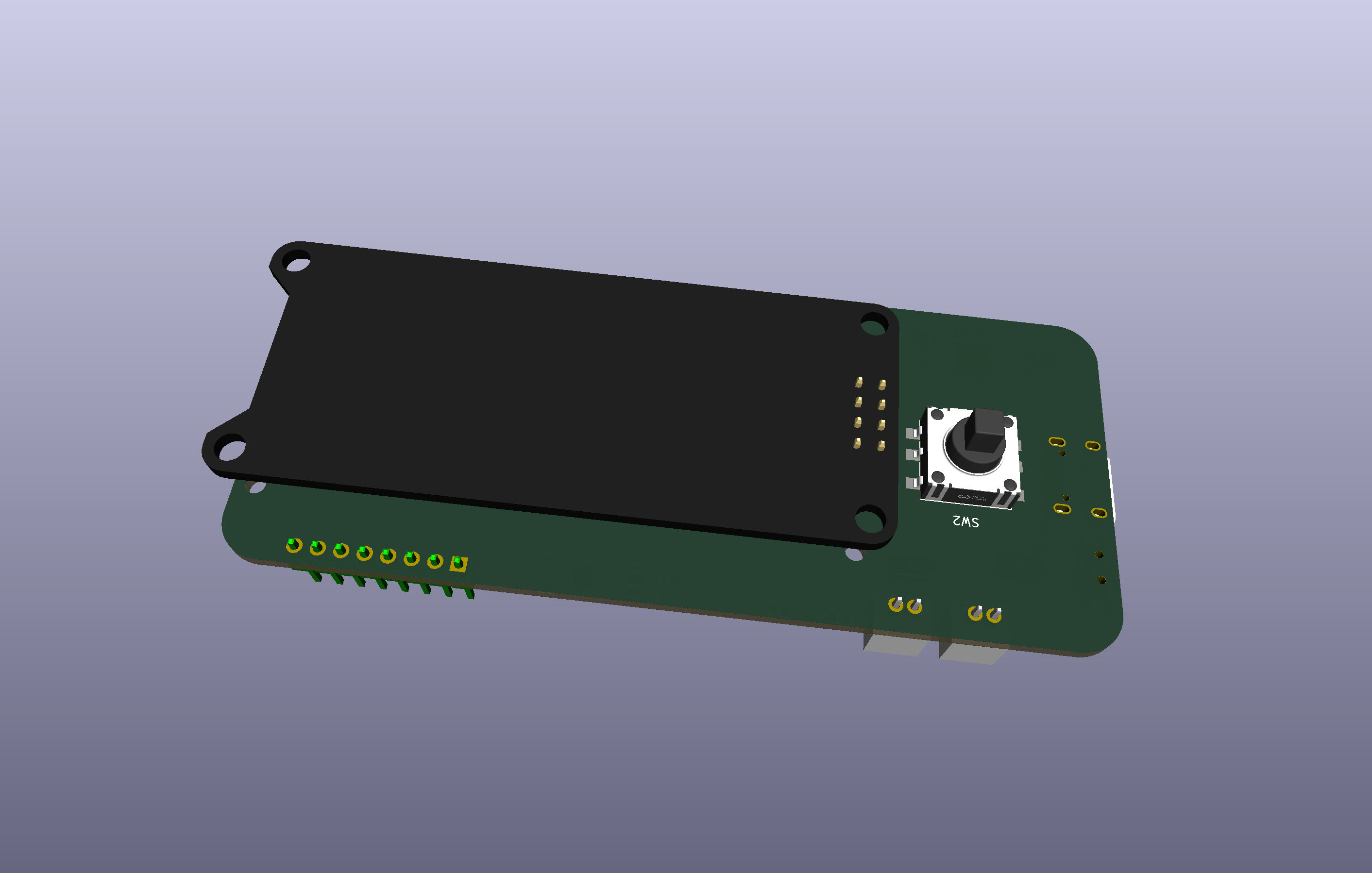
The back hosts the 5-way joystick switch (so the thumbpiece sticks out the back of the case), the JST connectors for the solar panel and the battery, and a chunky little debug header that mirrors the e-paper's SPI lines.
The steps to get here
The journey was less "draw a circuit" and more "play detective across a stack of reference designs." Here is the friendly version of the process.
1. Decide what's actually on the board
I almost started this whole thing from the BOM file. That was the wrong source. The BOM had old parts on it that the project had already moved past. The real source of truth turned out to be the FreeCAD model of the case — every body in the case is a real thing that has to land somewhere on the new board. If it's in the case, it's on the board. If it's not in the case, it doesn't exist yet.
So step one was reading the case, not the parts list.
2. Find a working reference for every part
Rather than design any component circuit from scratch, I went hunting through the repo's stash of reference projects. For every part the case needed, I tried to find a board that someone smarter than me had already built and proven:
- For the Pi Pico 2 W, the official Pico carrier-board project.
- For the TP4056 charger and battery protection, a tiny open-source charger board.
- For the gyro sensor on an I²C bus, an example sensor breakout that wires up multiple I²C chips cleanly.
- For the e-paper screen, an existing ESP32 e-paper carrier with the SPI signals already named.
- For the joystick footprint, my own Rev 2 joystick PCB from last month (which finally has the right pad layout).
Eleven reference projects in total — all openable directly in KiCad, all already proven by someone else.
3. Wire it up in KiCad
The schematic is where you draw the logical picture — boxes for each part, lines between their pins, names like SDA, SCL, EINK_CS, BTN_UP showing how things connect. This is the wiring diagram side of the work.
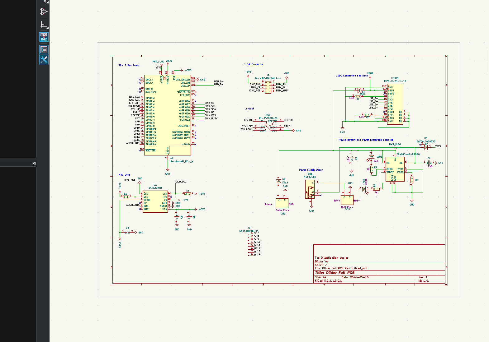
The schematic was built sheet by sheet to mirror the case: a sheet for the Pico, a sheet for power, a sheet for the screen, a sheet for the sensors, a sheet for the buttons and joystick. Each one wires into the next via named labels — like little teleporters that say "this SDA is the same SDA over there."
4. Lay it out on a real rectangle
Once the schematic was right, the layout work began — taking that logical wiring picture and turning it into a physical 3D object. Every component gets dragged onto a green rectangle the size of the inside of the case, then every signal gets a copper wire ("trace") drawn between its pins. KiCad shows ghostly lines for the connections that aren't routed yet, and slowly, one trace at a time, you replace each ghost line with real copper.
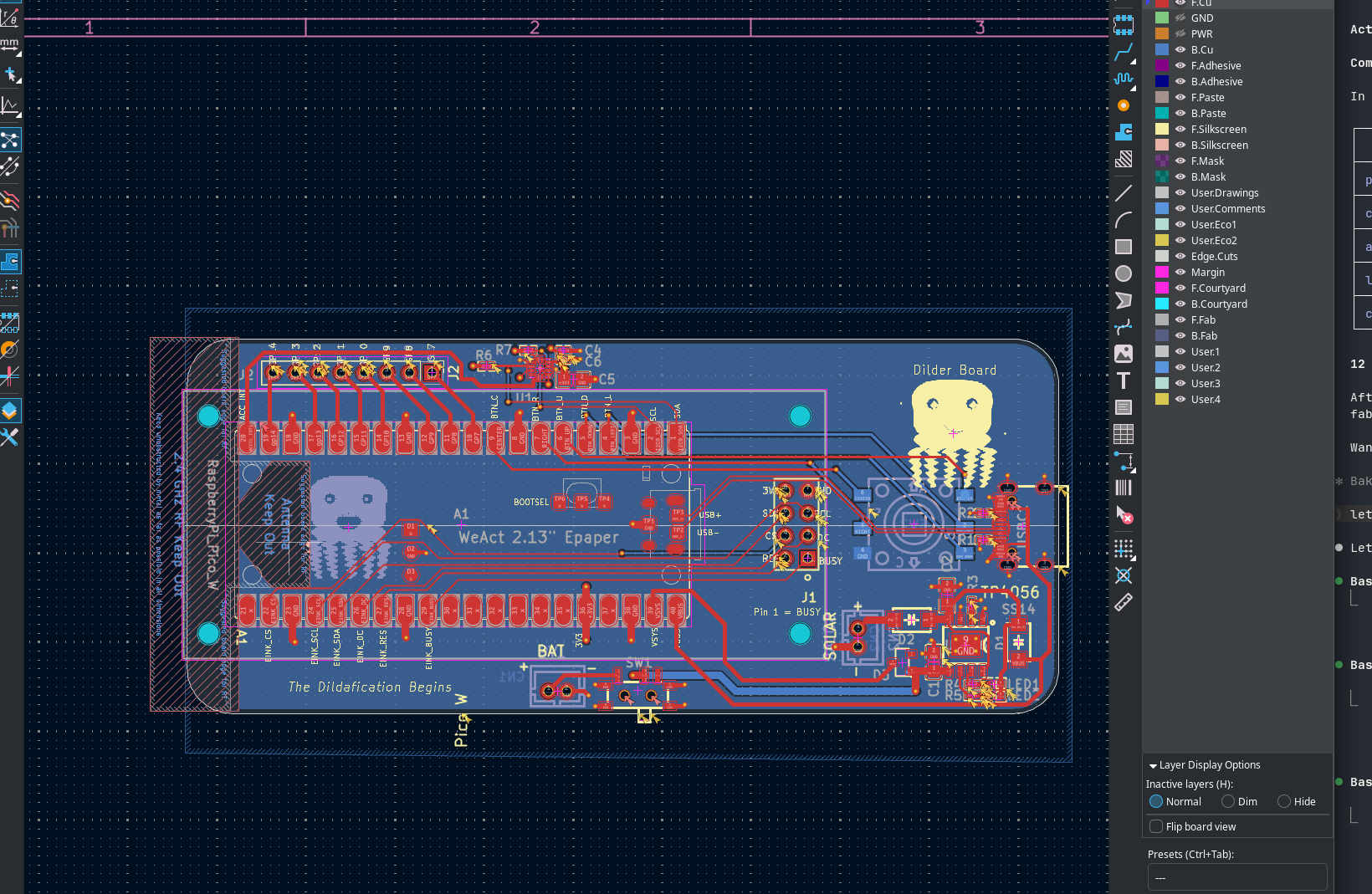
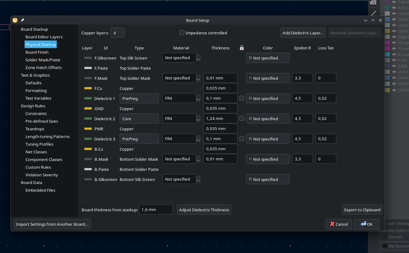
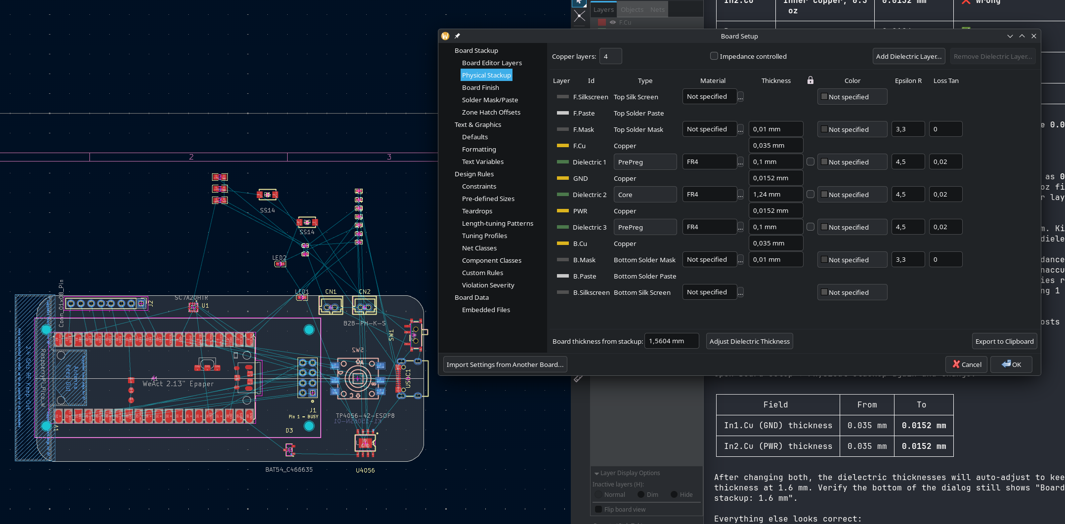
5. Set up a real 4-layer board stack
Most cheap hobby PCBs are 2-layer — copper on the top, copper on the bottom, fibreglass in the middle. This board is 4-layer, which means two extra copper sheets sandwiched in the middle: one is a solid ground plane, the other is a solid 3.3 V plane. That makes signal routing easier (you almost never have to dodge a power wire) and keeps the board electrically quieter.
6. Check the 3D preview
KiCad's most rewarding feature is the 3D viewer — once everything is routed, it renders the finished board as if you were holding it. This is the moment where weeks of clicking turns into a real-looking object.
7. Test fit the screen
The final visual check — does the e-paper screen still fit where the case says it should? Spoiler: yes.
What this milestone really means
Up to now, every Dilder unit has been a small forest of jumper wires inside a 3D-printed shell. Rev 1 of the Full Board is the moment where the project stops being a "breadboard with a case around it" and starts being an actual hardware product.
That's a big deal for two reasons:
- The case can shrink. Once the wires are inside the board, the case doesn't need internal channels for them anymore. The next case revision can be measured against the board, not the bag of modules.
- Building another one becomes realistic. Sending this file off to a fab, getting five boards back, and handing one to a friend is now a one-shot affair rather than an afternoon of soldering rainbow ribbon.
What's next
A few clear next steps:
- Order the board. Send the Gerbers off to JLCPCB and get the first batch of physical boards in hand.
- Solder the extended components. The fancier surface-mount parts (USB-C connector, TP4056 chip, IMU sensor, slide switch, decoupling capacitors) get hand-soldered onto the bare boards once they arrive.
- Design a new FreeCAD case around it. Now that the board is the new fixed shape, the case has to be re-measured and re-modelled around it — slimmer, smarter, with no leftover rails for modules that no longer exist.
It took two months of breadboards, dozens of FreeCAD prints, and eleven reference designs to get here — but the board is real, the silkscreen is checked, and the dildafication has officially begun.